High-Performance Sapphire RV32 SoC
The high-performance hardened Sapphire RV32 SoC provides interfaces to support a variety of peripherals, e.g., memory controller, direct memory access channel, custom instruction, and I/O devices. You can choose the interface you want to use by configuring the SoC in the Efinity® IP Manager.
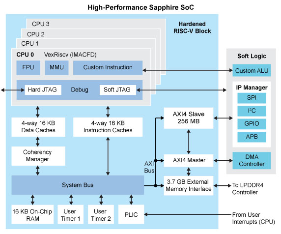
- 4 VexRiscv processor(s) with 6 pipeline stages (fetch, injector, decode, execute, memory, and write back), interrupts and exception handling with machine mode
- Up to 1 GHz system clock frequency
- 16 KB on-chip RAM with boot loader for SPI flash
- Memory controller for LPDDR4x
- Supports memory module sizes of 3.7 GB
- User-configurable external memory bus frequency
- 1 full- duplex 512-bits AXI4 interface to communicate with the external memory
- 1 AXI master channels for user logic, data widths of 128-bits
- 1 AXI slave channel to user logic
- Each core includes:
- 4-way 16 KB data and instruction caches
- Floating point unit (FPU)
- Linux memory management unit (MMU)
- Custom instruction interface with 1,024 IDs to perform various functions
- Supports RISC-V extensions such as integer, multiply, atomic, compressed, single, and double-digit floating point.
- JTAG debug module with 8 hardware breakpoints
- Peripherals:
- 2 user timers
- 24 user interrupts
This SoC is only available in selected FPGAs, refer to the Titanium and Topaz for details on which devices are supported.
Read data sheet >
Sapphire RV64 SoC
The Sapphire RV64 SoC extends the Sapphire RV32 SoC architecture with enhanced cache configurations, expanded memory bus capabilities, and flexible I/O options for greater performance and scalability.

- 1 - 4 (user selectable) VexiiRiscv processor(s) with 7 pipeline stages (fetch, align-decompress, decode, issue, execute, memory, and writeback), interrupts and exception handling with machine and supervisor modes
- 20 – 400 MHz system clock frequency
- 4 - 512 KB on-chip RAM with boot loader for SPI flash
- Debug:
- Supports standard RISC-V debug specification
- Up to 4 hardware breakpoints
- Up to 4 performance counters
- Supports co-debug with the FPGA debugger
- Memory controller for DDR3, LPDDR4x or HyperRAM memories, supports memory module sizes from 4 MB to 8 GB:
- User-configurable external memory bus frequency:
- 1 half- duplex AXI3 interface (up to 512-bits) or 1 full-duplex AXI4 (up to 512-bits) to communicate with the external memory
- 400 MHz DDR3 clock frequency, 800 Mbps
- 1,600 MHz LPDDR4x clock frequency, 3,200 Mbps
- 250 MHz HyperRAM clock frequency, 500 Mbps
- Up to 2 AXI slave channels for user logic, data widths from 32 to 512-bits, with memory coherency
- 1 AXI master channel to user logic
- Includes a multi-way L1 instruction and data cache
- Includes an optional L2 cache
- Includes an optional branch predictor
- Includes an optional physical memory protection unit
- Includes an optional hardware and software pre-fetcher
- Includes a floating-point unit (FPU)
- Includes an optional Linux memory management unit (SV39 MMU)
- Includes an optional custom instruction interface with 1,024 IDs to perform various functions
- Supports optional RISC-V extensions such as single and double-digit floating point, atomic, compressed, bit manipulation, and cache block management
- I/O peripherals:
- Up to 32 GPIOs
- Up to 5 I2C masters
- Clint timer
- Platform-level interrupt controller (PLIC)
- Watchdog timer
- Up to 3 SPI masters
- Up to 3 user timers
- Up to 3 UARTs with 115,200 baud rate
- Up to 5 slave user peripherals with APB3 interface
- Up to 8 user interrupts
This SoC is available for all Trion® FPGAs (except the T4 and T8), all Titanium® FPGAs, and Topaz® FPGAs.
Read data sheet >
Sapphire RV32 SoC
The Sapphire RV32 SoC is a general-purpose, user configurable, soft core SoC that supports a wide variety of embedded applications.
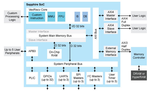
- 1 - 4 (user selectable) VexRiscv processor(s) with 6 pipeline stages (fetch, injector, decode, execute, memory, and write back), interrupts and exception handling with machine mode
- 20 – 400 MHz system clock frequency
- 1 - 512 KB on-chip RAM with boot loader for SPI flash
- Memory controller for DDR3, LPDDR4x or HyperRAM memories
- Supports memory module sizes from 4 MB to 3.5 GB
- User-configurable external memory bus frequency
- 1 half- duplex AXI3 interface (up to 512-bits) or 1 full-duplex AXI4 (up to 512-bits) to communicate with the external memory
- 400 MHz DDR3 clock frequency, 800 Mbps
- 1089 MHz LPDDR4x clock frequency, 2178 Mbps
- 250 MHz HyperRAM clock frequency, 500 Mbps
- Up to 2 AXI master channels for user logic, data widths from 32 to 512
- 1 AXI slave channel to user logic
- Includes an optional multi-way Instruction and Data Cache
- Includes an optional Floating Point Unit (FPU)
- Includes an optional Linux Memory Management Unit (MMU)
- Includes an optional custom instruction interface with 1,024 IDs to perform various functions
- Supports optional RISC-V extensions such as atomic and compressed
- APB3 peripherals:
- Up to 32 GPIOs
- Up to 3 I2C masters
- Clint timer
- Platform-Level Interrupt Controller (PLIC)
- Up to 3 SPI masters
- Up to 3 user timers
- Up to 3 UARTs with 115,200 baud rate
- Up to 5 slave user peripherals
- Up to 8 user interrupts
This SoC is available for all Trion® FPGAs (except the T4), all Titanium® FPGAs, and Topaz® FPGAs.
Read data sheet >
Sapphire RV32 Lite SoC
The Sapphire RV32 Lite SoC has the smallest footprint and is ideal for microcontroller applications. In its smallest variation, it uses fewer than 4K LEs. This slimmed down version is ideal when you need just a little bit of processing power.
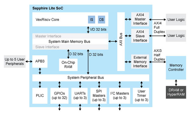
Supported Features
- Single-core soft VexRiscv processor (RV32IM) with 6 pipeline stages (fetch, injector, decode, execute, memory, and write back), interrupts and exception handling with machine mode
- Optimized for area, can go lower than 4K LE
- Customizable on-chip RAM, cache, and APB3 peripherals
- Ablility to run FreeRTOS
- 1 half- duplex AXI3 interface (up to 512-bits) or 1 full-duplex AXI4 (up to 512-bits) to communicate with the external memory
- 0.7 DMIPS/MHz with internal memory
Limitation
- No custom instruction
- No Atomic extension
- No Compressed extension
- No FPU
- No MMU (no Linux support)
This SoC is available for all Trion® FPGAs (except the T4), all Titanium® FPGAs, and Topaz® FPGAs.
Read data sheet >