AI and FPGAs

Among all the possible computing applications that can require massive levels of processing power, artificial intelligence is arguably near the top of the list. The level of computing power required to build some artificial intelligence models using conventional processor architectures can be massive. Some training tasks use so much data and require extensive preprocessing, and the level of computing power needed to implement these tasks in reasonable timeframes is only available in a cloud-connected data center.


At the other end of the AI computing spectrum are inference tasks, some of which are computed rather quickly in smaller neural network architectures. Furthermore, with a highly optimized, highly specific AI model trained against a carefully chosen dataset, the level of compute required for inference can be greatly reduced to the point where reliance on the cloud is not necessary. Much of the recent work in the software world and in the research literature has focused on optimizing neural network architectures for very specific tasks so that inference and training tasks are accelerated.

While AI has long been the domain of software developers, the electronics industry has worked to move AI compute capabilities onto embedded systems with unique chipsets, model optimization, and even unique transistor architectures that mimic analog circuits. Today and going into the future, the focus has and will continue to shift towards performing AI tasks on end-user devices with powerful embedded processors. FPGAs are some of the best contenders for implementing AI compute on embedded devices, but without the need for unique custom silicon.

Challenges in Embedded AI

Moving AI tasks away from the data center and onto an end device has the potential to enable a whole new range of computing applications. Industries like robotics, security, defense, aerospace, healthcare, finance, and many more are implementing AI compute capabilities. However, new products in these areas continue to require a constant connection back to the cloud, or at least to an edge server, to implement the basic data preprocessing, inference, and training steps required in any AI-capable system.

AI is High-Compute

AI processing is computationally intensive, therefore many production-grade services involving AI require training and inference in a data center. These existing services and applications are largely software driven, providing services and experiences to users through a platform or end devices over the internet. Portions of these services are very high compute, particularly training, although inference in some tasks can involve comparably large datasets processed in parallel.

AI computation on a small device can also require significant computing power, especially when adapted to applications like vision and sensor fusion. Embedded AI capabilities have recently become available by effectively attempting to mirror the compute architecture used in data centers and miniaturize it on an end device, or by adding a single accelerator chip that provides small-scale AI training and inference capabilities. GPU products from semiconductor vendors and small accelerators have been available for some types of AI applications, but these can be very bulky and inefficient (for GPUs) or highly specified (for accelerators).

Real-Time AI Requires Low Latency

Some AI applications require low latency, so they can’t perform inference in the data center. The time required to transmit data from the end device, have it processed in the cloud, and return results to the end device, may be too long for some advanced application areas. Similarly, tasks like training against large datasets, such as those that might be aggregated from a network of distributed devices, may take too long to perform on the end device and are best done in the cloud. Those tasks that are time-critical should be performed on the end device that act on the results from an AI inference model.

To solve this problem, a cloud or edge connection can be relied on for higher-compute training tasks involving very large datasets, while faster inference tasks should be performed on an end-user device or embedded system. For these systems, getting production-grade vision capabilities to run in real time on an end device has been challenging with current chipsets. An alternative system architecture is needed for time-critical inference and data pre-processing on an embedded device.

Separating Inference and Training

Between inference and training, inference is a lower compute task that only requires a single input dataset. Pre-processing may be required on captured data or collected signals, but this is generally much less computationally intensive than inference. As a set of successive multiply-add operations, simple neural network models can be implemented on an embedded processor (MCU/MPU) and used for inference computation within reasonable timeframes.

In contrast, training is much more data intensive, requiring significant compute resources when implemented in production-grade AI-capable systems. Even for a small dataset and small neural network architecture, the computational expense of training can be difficult for some embedded chipsets to implement quickly. The compute resources required for training might be available in the cloud, but not on every end-user device. The desire for an all-in-one solution to training and inference at the edge has helped drive development of accelerator chips, GPU solutions, and cloud infrastructure to support on-device AI.

The Embedded AI Landscape

All systems that implement AI capabilities need to balance the need for on-device compute and access to peripherals.

Embedded AI Chipset Options

The current range of chipsets that can support certain embedded AI tasks with acceptable latency looks very familiar to most engineers. These include:

MCU photo
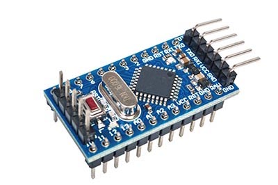
Microcontroller (MCU)

These mainstays of embedded computing are suitable for some AI inference tasks and training against smaller datasets. Some semiconductor vendors provide developer resources and libraries that allow model quantization to speed up simpler inference tasks.

MPU photo
Microprocessor (MPU)

These processors scale up the capabilities available on MCUs to allow more complex pre-processing and training against larger datasets as long as the system architecture can support it. Inference may be faster on these devices as well thanks to faster clock speeds.

SoC photo
AI Accelerator

These chips are highly specific and will implement a compute architecture that is optimized for specific AI inference tasks. Accelerators are available for inference with short voice streams or still images as long as a trained neural network model is available. Parallelization is limited with these devices, which may require multiple accelerators in the same system.

GPU photo
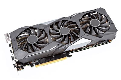
Graphics Processing Unit (GPU)

These processors are often used for AI training and inference in data center settings, or in rugged embedded computing settings such as in industrial and aerospace systems. Smaller GPUs are available that can be deployed on an embedded device, most notably on a single-board computer or module.

FPGA photo
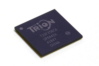
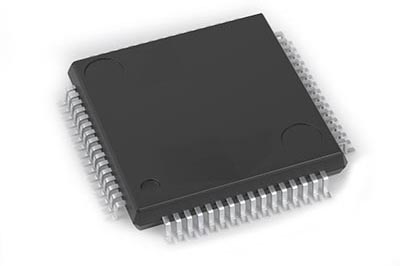
Field-Programmable Gate Array (FPGA)

These programmable logic devices allow implementation of a totally custom compute architecture. AI-specific accelerator blocks can be implemented that are optimized for specific AI tasks. The compute architecture in these devices can also be highly parallelized, something which is not possible in other devices.

Among these devices, FPGAs are the most adaptable, most customizable options for incorporating AI capabilities into an embedded system. The industry is now realizing this, and new MCU/MPU components that incorporate an FPGA-based processor block are being produced by major semiconductor manufacturers. These additional processor blocks are being added specifically to address the demand for AI capabilities on an embedded device.

The next natural step for a systems designer is to just use an FPGA as the main system host controller, where everything needed to run a system is instantiated in the FPGA. A similar option is to place an FPGA as an additional component, which can then be used as an accelerator and interface controller while the main chipset can be a conventional MCU/MPU. While the FPGA development effort can be significant for some designers, FPGAs provide many benefits that are not found in other processor architectures.

Benefits of FPGAs in AI Systems

In each of the above application areas, the use of an FPGA is providing very specific benefits in an edge compute application:

  • Fully reconfigurable logic allows repeated updating of logic architecture to fully optimize AI inference and training
  • Optimized logic architecture minimizes power consumption by eliminating unused interfaces and repetitive add-multiply-shift operations in traditional architectures
  • Highly parallelizable logic can be implemented to speed up AI inference, even with very large input data sets
  • Vendor IP can be used to instantiate multiple high-speed interfaces that receive sensor data or digital data from other components
  • AI can be implemented on top of a standard SoC core like RISC-V, which can support an embedded OS and user applications
  • FPGA footprints can be comparable to or smaller than traditional processors or AI accelerators
  • Universal configurability of FPGAs reduces supply chain risk and allows instantiation of external components in the system logic

For AI applications built on top of FPGAs and vendor IP, systems designers can deploy a new AI-capable system quickly with a fully optimized, fully reconfigurable architecture. Continuous system reconfiguration is essential in AI as neural networks are continuously retrained and redeployed to the embedded processor. By continuously optimizing the system’s logic architecture, power consumption and processing time can be kept as low as possible. This is not possible with accelerators that have a static logic architecture.

Where FPGAs Excel in AI

For AI inference tasks on the end device, or as an acceleration element in a data center or another component, FPGAs are being used in a variety of systems and application areas:

Application Characteristics
Vision systems FPGAs are an excellent replacement for GPUs in vision systems; they can implement tensor computations in parallel, but in a smaller package with less power usage. FPGAs can also instantiate the required vision interfaces, DSP, and embedded application directly in silicon, whereas a GPU requires an external processor and high-bandwidth PCIe interface to receive vision data.
Sensor fusion Because FPGAs can have high I/O counts for multiple digital interfaces, they are a preferred platform for sensor fusion. FPGA-based systems can capture multiple data streams, implement on-chip DSP, and aggregate data into an on-chip inference model as part of a larger application. This is all done in parallel, making it much faster than MCU/MPU computation. Compared to GPUs, this happens on a much smaller footprint with less power.
Interoperable systems Industrial systems and mil-aero are two areas where interoperability between diverse system elements can be achieved with FPGAs. With FPGAs being reconfigurable and allowing customization of interfaces, they can be used as the primary processor element in distributed systems requiring interoperability. This also allows FPGAs to be used in legacy systems that cannot be easily upgraded with newer components; the FPGA is simply adapted to interface with the existing system.
Wearables and mobile Small wearables and mobile devices are another area where system miniaturization is at odds with increasing feature density. FPGAs are advantages here as they allow feature density to be increased with new AI capabilities that are not possible on MCU-based systems. These systems may also not have room for an AI accelerator, but this could be implemented with an FPGA as the main processor.
5G and telecom It is often said that 5G will be a great enabler of embedded AI, but low-latency AI-enabled applications requiring 5G connectivity can only be implemented with an appropriately fast chipset. FPGAs can play a role here as a heavily optimized accelerator element deployed in the data center, at the edge, or on an end-user’s device. A reconfigurable AI accelerator like an FPGA would be key to service delivery demanded by 5G users.
Add-in acceleration FPGAs have already been used as dedicated AI acceleration elements in data centers and edge servers as add-in modules. The same functionality can be implemented on smaller embedded devices with SoC IP provided by some semiconductor vendors. Further acceleration is also possible at the firmware or model level with TensorFlow Lite and open-source libraries.

FPGAs can be used in multiple ways in the above application areas, such as the primary processor in smaller devices or as a dedicated accelerator for larger systems. For legacy systems, it’s possible for FPGAs to be used as an add-in element that provides the required AI capabilities with minimal system overhead. From the application areas listed in this table, the main advantages of FPGAs are reconfigurability, customization, and I/O count with high-bandwidth options available.

AI

FPGAs in AI Systems and Network Architectures

The system and network architecture used to facilitate AI inference and training with FPGAs will dictate which tasks are feasible on the end device, and which might need to be offloaded to the edge or the cloud. In the case of an accelerator card deployed in a data center or an edge server, it’s important to consider the level of compute required for application execution and service delivery. This can then dictate the size of the FPGA (both physical and logic cell count) that is used in the deployed system.

System Architecture

FPGAs can occupy two possible roles in an embedded system requiring AI compute capabilities:

  • Main processor, where a core architecture and an embedded OS are instantiated in hardware. When minimal component count is needed and extraneous compute operations can be eliminated, this is the best path forward for design with an FPGA that includes AI compute.
  • Co-processor, where the FPGA is used as an external accelerator to support a main processor (MCU or MPU). The FPGA used in this case does not need to instantiate a core or run an operating system, it only needs to instantiate highly specified AI compute operations in the interconnect fabric.

As a main processor element, larger FPGAs might be needed to support an embedded OS and any applications required to implement the required system functionality. As a co-processor, the size of the FPGA will depend on the compute density and parallelization needed in the embedded AI compute architecture. In either case, the FPGA can be used to reduce total component count by instantiating logic from other ASICs in the FPGA interconnect fabric.

Any external features not required for time-critical AI compute can be accessed through an edge or cloud resource. The above implementation does not necessarily require a cloud connection for any AI inference tasks, and the product could be used as a standalone device. When model updates are needed, a connection to a cloud service or edge computing resources can be useful as this gives developers access to additional compute for training, web access, remote storage, and service delivery. The role of an FPGA-enabled device within a larger network may also affect how the end device is built and developed.

AI-Enabled FPGA Development

After selecting an FPGA product that can provide the required I/O count, logic cell count, interfaces, and latency, the FPGA architecture needs to be streamlined to ensure minimal processing overhead in AI compute tasks. Vendor IP can be used to accelerate core implementations, interface implementation, and logic development in their IDE. RISC-V is a natural ISA to begin developing an FPGA with AI compute capabilities as it can be highly customized, and some vendor IP supports RISC-V implementations to help users quickly build a new AI-enabled system.

At a high level, the FPGA development process proceeds through the following steps:

  1. Select an FPGA and vendor IP to instantiate a core architecture and instruction set
  2. Implement custom logic with IP using vendor developer tools
  3. After simulation and verification, compile the application to a HEX file
  4. Programming the FPGA, followed by testing and debugging on an evaluation product
  5. Based on testing results, modify the application code build a custom board for the end product
  6. Prototype with a custom board to ensure support for any required peripherals
  7. Adjust the application to address any outstanding problems found during testing and prepare for production

For AI development, it’s possible to leverage open-source projects and libraries to accelerate product development. TensorFlow Lite can be used in C code to build an application on top of the core application. Before you select an FPGA product for embedded AI, make sure your vendor supports cutting-edge open-source toolsets and libraries like RISC-V and TensorFlow Lite as these can help accelerate logic development and computation on the end product

.

AI in FPGAs with Efinix

Semiconductor vendors are realizing the advantages of FPGAs used for AI acceleration or as an entirely customizable SoC in advanced embedded systems. Efinix is one company that sits at the forefront of AI implementation in FPGAs targeting high-compute requirements in the cloud or edge, as well as low-latency AI tasks on embedded devices. Through an extensive portfolio of SoC IP based on RISC-V implementations, Efinix customers can accelerate system development and deployment with powerful AI capabilities without the need for custom silicon or accelerators.

Product Lines

Efinix’s two FPGA product lines can support RISC-V implementations that target high compute density applications. The Titanium and Trion FPGA lines target a range of logic cell requirements with high compute density and multiple interfaces for advanced applications. Multiple part numbers are available with various package sizes and interfaces included on the device.

Titanium FPGAs

Titanium Logo

The Titanium line of FPGAs are larger components for more advanced applications requiring greater logic capacity and I/O count. These devices are built on a similar architecture as Trion components, but these products have broader support for standard data/memory interfaces. For streaming applications involving low-latency AI and communications with other systems, Titanium devices support SerDes interfaces with high data rate.

  • Up to 1M logic cells
  • 4-lane MIPI, DDR4/LPDDR4, up to 25.8 Gbps SerDes, PCIe Gen4 interfaces supported
  • DSP block optimized for high compute applications like AI
  • Efinix RISC-V core with integrated audio and vision interfaces
  • Ideal for high compute industrial systems, larger vision products, and edge AI applications

The Titanium FPGA provides much larger logic cell count and additional interfaces that are instrumental in embedded AI systems. This makes the Titanium a better fit for heavier AI inference workloads in an end device, or for training in a range of neural network architectures. This product is also large enough to act as a main system controller with embedded AI capabilities implemented on top of the core architecture

Trion® FPGAs

Trion Logo

The Trion FPGA is a physically smaller device that offers the same compute capabilities as a larger FPGA, MCU, or MPU. These devices are ideal for smaller embedded systems implementing AI inference with multiple data streams. These devices have high I/O count, high logic cell count, and standard integrated interfaces and will support additional high-speed interfaces required in high compute applications:

  • Up to 120k logic cells
  • 4-lane MIPI, LVDS, and up to DDR3/LPDDR3 interfaces supported
  • Dedicated interface block
  • Efinix RISC-V core with integrated audio and vision processing
  • Ideal for mobile/IoT products, smaller vision products, and AI inference applications

Vendor IP for the Trion FPGA includes RISC-V-based SoCs that allow the Trion FPGA to be used as a standalone processor or as a dedicated AI accelerator. The IP and development libraries available from Efinix, as well as open-source AI toolsets, can be leveraged to build a highly optimized reconfigurable AI-capable embedded system with small footprint and low power consumption.

RISC-V Implementations for Embedded AI

Every processor requires an instruction set architecture (IAS) that defines how logic operations are to be constructed and executed in real digital logic circuits. RISC-V is one such ISA that has many advantages in applications like embedded AI, where a highly streamlined computing architecture is required to ensure maximum efficiency. RISC-V is an open-source ISA that can be totally customized and implemented on an FPGA

.

Efinix offers a set of SoC IP based on RISC-V to help customers quickly create and deploy hardware implementations Titan and Trion products. The main features in this development library include:

  • 32-bit CPU using the RISCV32I ISA with extensions, and pipeline stages
  • Library includes a configurable feature set with user peripherals (SPI, I2C, etc.) on an APB bus
  • RISC-V processor, memory, multiple high-speed I/Os, customizable interfaces, and memory controllers on an AXI bus

Efinix’s variants of its standard RISC-V library are the Sapphire and Edge Vision SoCs. These RISC-V-based cores from Efinix provide a highly integrated SoC that is optimized for low power consumption and high compute density that is demanded in embedded AI systems. This SoC can be ported over to a Linux kernel (Yocto) to support embedded applications, as well as dedicated logic blocks for highly parallelized AI processing.

Sapphire SoC - This user-configurable, high-performance SoC includes 6 pipeline stages (fetch, injector, decode, execute, memory, and write back) with an optional memory controller (DDR or HyperRAM up to 3.5 GB), all running at moderate clock frequency. Support for standard and custom features can be integrated and managed in Efinix development tools. There is also extensive access to peripherals with multiple interfaces (up to 32 GPIOs, 3 I2C masters, 3 SPI masters, and 3 UARTs).

Edge Vision SoC - This SoC library tailors an Efinix FPGA for vision applications with all buses, controllers, and interfaces included in the development library. Additional user functions and instantiation of specialized processing blocks can also be implemented at a system level as well as RISC-V acceleration at the instruction level. The goal of this accelerator implementation is to facilitate hardware/software partitioning with specific functions applied to streaming vision data, all operating at low latency.

Both SoC libraries are accessed and configured in the Efinity IDE while configuring Trion or Titanium FPGAs. Users can also tailor their AI workflow and model implementation in this development environment, as well as customize their core and interface requirements.

Efinity IDE - The Efinity IDE is Efinix’s development environment for Titanium and Trion FPGAs. Efinity provides a complete environment for developing RISC-V implementations for Efinix FPGAs, including standard and user-defined extensions. With access to the Sapphire and Edge Vision SoC libraries, users can design their RISC-V based implementation in the Efinity GUI or with built-in command-line scripting support. Some of the major development features of the Efinix IDE include:

  • Project management dashboard
  • Interface and floorplan design tool for logic design, pin assignment, and routing
  • Timing analysis features to analyze and optimize device performance
  • Hardware debuggers for logic analysis
  • Simulation support with ModelSim, NCSim, and iVerilog simulators

1-year licenses are available to customers who purchase a development kit. The license includes one year of upgrades and a free maintenance renewal is available upon request.

Acceleration With TensorFlow Lite

Increasingly quantization methods are being used to push inference out to the extreme edge targeting microcontroller platforms. Unfortunately the limited compute capability of microcontrollers often results in poor system performance. Leveraging the custom instruction capability of the Efinix Sapphire RISC-V core, it is a trivial job to replace the software primitives of the TensorFlow Lite quantized model with highly accelerated hardware instructions. Hardware acceleration of 500X can easily be achieved relative to the software only implementation. Leaving the majority of the model in software and implementing just a few custom instructions to achieve the desired performance results in rapid time to market with an intuitive software defined flow.

The hardware / software partitioned approach is typical of the benefits afforded by FPGAs where system control can be implemented in sequential software code while performance critical elements can be accelerated in parallel, deterministic hardware accelerators. Only a few lines of VHDL code are needed to implement custom instructions making the approach realizable for design engineers that are more familiar with software only flows. This TinyML based approach is available free of charge in the Efinix TinyML framework and can be downloaded from the Efinix Github. The TinyML framework contains example flows, reference custom instructions and fully implemented models as a starting point for designers implementing their own AI applications.

Why Efinix?

Efinix has partnered with a broad range of customers and focuses its product lines on applications requiring high compute in small form factor devices. Its customers are innovative industrial, consumer, medical device manufacturers, or high-end automotive companies. Ideal applications include vision, sensor fusion, and on-device AI/ML in these markets. The low power consumption and small footprint of Efinix’s flagship products make them perfect for surveillance or industrial automation applications.

Efinix customers tend to require a tailored small form-factor FPGA solution that helps eliminate significant R&D costs while still allowing product customization and reconfiguration. The RISC-V SoC libraries are instrumental for Efinix customers as they help expedite creation of new designs and reduce time to market.

Developers that want a faster path to market with an alternative option to larger FPGA platforms can leverage the significant developer resources and powerful compute capabilities provided by Efinix FPGAs. As a smaller company, Efinix takes a high-touch approach that leads to longer-term relationships and innovative FPGA applications.

Get Started with Efinix

To get started with Efinix FPGAs, take a look at our development kits and developer resources.