Designing with FPGAs
If you’ve decided that an FPGA is the optimal solution for your product, you can begin moving through the design process for your FPGA. The process begins with selecting the appropriate architecture for your system, followed by matching your system architecture and functional requirements to a commercially available FPGA. Your vendor’s level of support can also influence your decision of FPGA selection, and you should ensure they have an IP portfolio that can meet your needs.
System Architecture Overview
As we’ve seen in previous sections of this guide, there are multiple architectures where an FPGA can play an important role. Some possible uses are shown below.
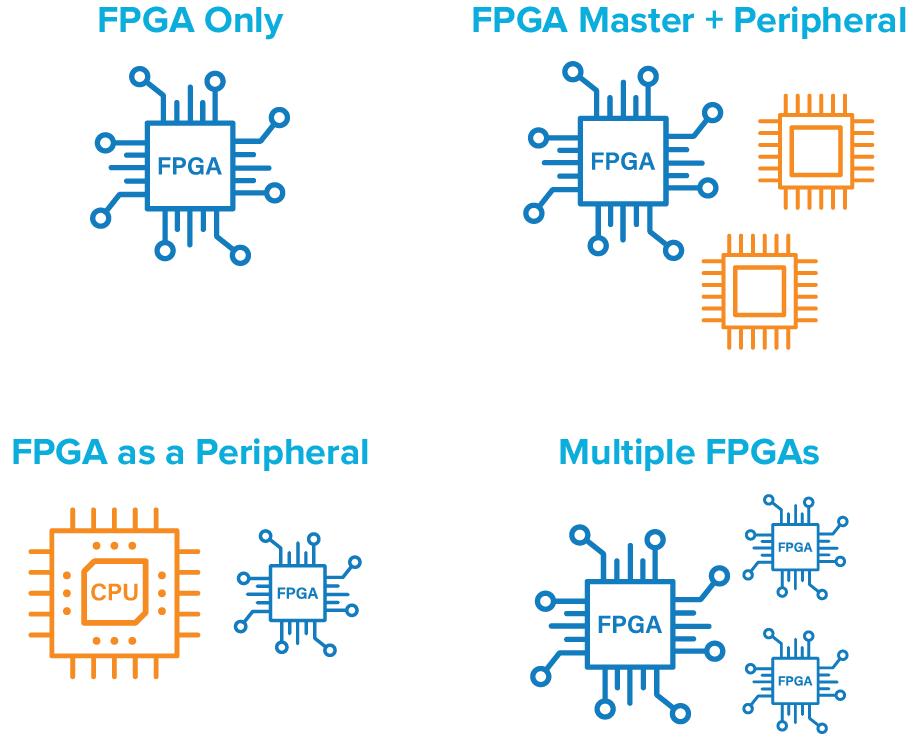
These are not the only options for integrating an FPGA into an embedded system. However, each of these should illustrate the adaptability of FPGA-based solutions: they can act as peripherals, main system controllers, or an integrated processor with few peripherals. Depending on the IP available from your FPGA vendor, you may be able to totally eliminate peripherals and instantiate everything in silicon, giving a much faster pathway to deploying a highly integrated SoC.
No matter how you choose to use an FPGA, its place in the system architecture and the functions it must provide will dictate the hardware requirements of your component. Importantly, this drives selection of the required I/O count, logic cell count, and IP that will be instantiated in the FPGA.
How to Select an FPGA for Your System
There are several important dimensions that should form the basis for FPGA selection.
I/O Count - This is the simplest place to start looking for an FPGA that can meet the needs of advanced embedded systems. The total number of I/Os is essentially the number of signals that can be accessed or sourced by the FPGA during operation. Physically larger FPGAs tend to have higher I/O counts. This is not often something you will have to calculate; FPGA vendors typically state a specific I/O count in their product datasheets.
If you took some time to build a functional block diagram for your system, and you’ve included interface information in your documentation, then it’s a simple matter to count up the number of I/Os the system will need and assign these to various interfaces.
Operating Frequency - In the most basic sense, this will tell you how fast the device can process a serial bit stream. Although faster clock rates do generally equate to faster processing, don’t be fooled by an FPGA with a slow clock. Processing in an FPGA can be done in parallel to a massive level, so even low clock rates can be used to implement logic operations and data processing in parallel with high data throughput. This type of customizable parallel processing is essential for large neural networks, vision applications, and sensor fusion.
Logic Cell Count - The basic building blocks of an FPGA are logic cells, and the quantity of logic cells is a measurement of the processing capacity available to the system. A device with more logic cells can generally accommodate more interfaces and more logic operations. Logic cell count will tend to scale with I/O count.
Memory - The amount of on-die memory available to an FPGA is extremely important for implementing modern applications. On-die memory embedded in the device interconnect fabric will be needed for logic operations, while external memory is normally accessed via a DDR interface. Less on-die memory available for logic operations will mean the device needs more external memory, which will consume some logic cells and I/Os to implement a memory interface.
Cost - Cost is a major factor that can drive FPGA device selection. If an FPGA will only be used in prototyping, or it will only be used in a one-off device, then cost of an FPGA component may not be a major consideration. Larger FPGAs (more logic cells and I/Os) will generally cost more because they can offer greater capabilities. Smaller FPGAs are finding a home in mass-produced devices that implement the advanced applications listed in earlier sections, so products produced at high volume can benefit from FPGAs from a cost perspective.
Vendor IP - An FPGA vendor’s IP portfolio exists to help developers quickly implement standardized interfaces in the device’s interconnect fabric. FPGA developers can rely on IP to instantiate interfaces required in their end product when programming their application. If IP for a standard interface is not available from the vendor or as open-source code, then it will have to be programmed from scratch. Available IP will target specific applications, and these should be considered when choosing between FPGA vendors.
FPGA Development Process
To get started developing a new application with an FPGA, the best place to begin is with a vendor’s evaluation product. FPGA vendors offer development boards for prototyping, testing, and debugging, so it is best from a risk perspective to start with a development product before deploying on a custom circuit board. Starting with an evaluation kit allows developers to eliminate potential defects on a custom board from their debug process and allows developers to focus on designing logic in the FPGA.
Vendor development products will also require access to an IDE for coding an application, compiling it to a HEX file/binary file, and programming this into the FPGA fabric. The process is similar to what is done with an MCU/MPU or an SoC. The main difference is that the “application” being coded is not stored in the device memory, it becomes instantiated in the device hardware.
At a high level, the FPGA development process proceeds through the following steps:
- Select an FPGA and any required vendor IP if available
- Implement custom logic with IP using vendor developer tools
- After simulation and verification, compile the application to a HEX file
- Programming the FPGA, followed by testing and debugging on an evaluation product
- Based on testing results, modify the application code build a custom board for the end product
- Prototype with a custom board to ensure support for any required peripherals
- Adjust the application to address any outstanding problems found during testing and prepare for production
Compared with MCUs or MPUs, IP provides an excellent way to work towards ready-made applications that still allow customization. Other programmable logic devices do not have this level of support and they may require total custom coding of all portions of an application. One common strategy is to combine libraries from multiple vendors into a single application, which is then compiled to a binary and flashed into the device’s memory. Vendor IP and developer resources can help designers circumvent these problems and reduce overall development time.
Before you start your next project, make sure you explore the hardware and IP options available from different vendors. The right FPGA vendor can help you quickly deploy a device that very closely matches your requirements thanks to their IP portfolio.
Meet Efinix
Efinix is an innovative FPGA vendor targeting edge, wearable, IoT, sensor, and machine vision markets. Efinix offers two FPGA product lines along with development resources to help engineers accelerate innovation and reduce time to market for FPGA-based products. Efinix offers two FPGA product lines:
Titanium FPGAs
A larger FPGA solution for more advanced applications requiring more logic capacity and I/O count. These devices are built on a similar architecture as Trion products with broader support for standard data/memory interfaces, as well as SerDes interfaces with high data rate.
- Up to 1M logic cells
- 4-lane MIPI, DDR4/LPDDR4, up to 25.8 Gbps SerDes, PCIe Gen4 interfaces supported
- DSP block optimized for high compute applications like AI
- Efinix RISC-V core with integrated audio and vision interfaces
- Ideal for high compute industrial systems, larger vision products, and edge AI applications

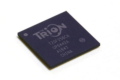
Trion FPGAs
A smaller FPGA option for embedded systems, these components take up small amounts of board space yet provide access to high I/O count and high logic cell count. These devices include standard integrated interfaces and will support additional high speed interfaces required in high compute applications:
- Up to 120k logic cells
- 4-lane MIPI, LVDS, and up to DDR3/LPDDR3 interfaces supported
- Dedicated interface block
- Efinix RISC-V core with integrated audio and vision processing
- Ideal for mobile/IoT products, smaller vision products, and edge AI applications
Developer Resources
To help FPGA designers start developing their Trion or Titanium FPGAs for popular applications, Efinix offers libraries that help designers quickly specialize their device for popular applications.
Efinity IDE - The Efinity IDE is Efinix’s development environment for Titanium and Trion FPGAs. Efinity provides a complete environment for working with Efinix FPGAs, design libraries, and IP with a GUI interface and command-line scripting support. Some of the major development features include:
- Project management dashboard
- Interface and floorplan design tool for logic design, pin assignment, and routing
- Timing analysis features to analyze and optimize device performance
- Hardware debuggers for logic analysis
- Simulation support with ModelSim, NCSim, and iVerilog simulators
1-year licenses are available to anyone who buys a development kit. The license includes one year of upgrades and a free maintenance renewal is available upon request.
RISC-V SoC - This development library allows users to implement a RSIC-V core in Titanium or Trion FPGAs. Based on the VexRISCV core, this development library provides high I/O count, user peripherals (SPI, I2C, etc.) on an APB bus, and high-speed interfaces and memory controllers on an AXI bus. The result is a highly integrated SoC that still enables the customizability of any other FPGA platform.
Edge Vision SoC - This development library tailors the RISC-V SoC to vision applications. The first-of-its-kind concept, this library includes all the buses, controllers, and interfaces needed in a typical signal processing ASIC for vision applications. Additional user functions and instantiation of specialized processing blocks can also be implemented with this library and Efinix’s other developer resources.
These FPGA silicon platforms are designed around the Efinix Quantum® fabric. The radically different architecture of the Quantum fabric eliminates wasted silicon and enables up to 4x area utilization compared to traditional FPGAs. This lets Efinix offer power and performance advantages over FPGAs from legacy manufacturers.
Why Efinix?
Efinix has partnered with a broad range of customers and focuses its product lines on applications requiring high compute in small form factor devices. Its customers are innovative industrial, consumer, medical device manufacturers, or high-end automotive companies. Ideal applications include vision, sensor fusion, and on-device AI/ML in these markets. The low power consumption and small footprint of Efinix’s flagship products make them perfect for surveillance or industrial automation applications.
Efinix customers tend to require a tailored small form-factor FPGA solution that helps eliminate significant R&D costs while still allowing product customization and reconfiguration. The RISC-V and Edge Vision SoC libraries are instrumental for Efinix customers as they help expedite creation of new designs and reduce time to market.
Developers that want a faster path to market with an alternative option to larger FPGA platforms can leverage the significant developer resources and powerful compute capabilities provided by Efinix FPGAs. As a smaller company, Efinix takes a high-touch approach that leads to longer-term relationships and innovative FPGA applications.
